Abstract
The thin film transistor liquid crystal display (TFT-LCD) is currently the most widely used liquid crystal display. This article introduces the basic information of TFT-LCD from its structure, principle, manufacturing process, characteristic index, research progress, and application.
Introduction
TFT-LCD technology is a high technology that combines microelectronics technology and LCD technology. By using microelectronic fine machining technology and Si material processing technology, people have developed the technology of growing Si materials on large-area glass plates and TFT planar array technology. Combined with the increasingly mature LCD manufacturing technology, product quality can be continuously improved, and the automatic large-scale production capacity can be enhanced. In addition, the qualified rate can be improved, the cost can be reduced, and its performance/price ratio can be closer to CRT.
1. The structure and working principle of TFT-LCD
A thin film transistor (TFT) liquid crystal display is an active matrix display formed by integrating a TFT switch into a twisted nematic (TN) liquid crystal display. This way, the shortcomings of passive matrix display, such as cross-interference, less information, and slow writing speed, can be overcome. And the display quality is greatly improved so that it can be applied to the high-resolution panchromatic display of computers and other fields.
The main component of the finished TFT-LCD is an LCD display module (LCM), which is composed of a Panel and a Backlight. As the core part of the whole liquid crystal display, the Panel has the most complicated manufacturing process. What people usually call bright spots are generated during the manufacturing process of the Panel. The quality of the backlight can directly influence the display effect, and it is usually the key factor influencing the life of TFT-LCD.
1.1 Structure and working principle of TFT-LCD Panel
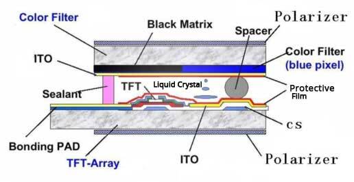
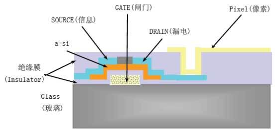
A TFT array is built on the glass substrate at the lower layer of the panel. The ITO electrode of each pixel is connected to the TFT drain electrode, the grid is connected to the scanning bus, and the original power supply is connected to the signal bus. When the scanning signal voltage is applied, the original source electrode is turned on so that the signal voltage is applied to the storage capacitor and charged. The signal voltage of the storage capacitor is applied to the liquid crystal pixel at the frame rate so that the liquid crystal pixel is in a gated state.
When addressing again, it is charged or discharged according to the signal voltage. In this way, each pixel is isolated by the thin film transistor switching element, which not only prevents cross interference but also ensures that the response speed of the liquid crystal can meet the requirements of the frame rate speed. Meanwhile, the gray level is obtained by the size of the stored source.
At present, the grayscale has reached 256 levels; that is, 16.7 million colors can be obtained (almost full-color display). Since the industry came into being in the 1990s, the production line of thin film transistor (TFT) liquid crystal display has developed from the first generation to the 11th generation. For each renewal of generation, the area of substrate glass has been greatly increased, the output continuously improved, and the cost continuously reduced.
Current mainstream TV sizes in the market: 32 inches (about 716 * 415mm), 39 inches (about 870 * 487mm), 43 inches (about 961 * 550mm), 49 inches (about 1090 * 621mm), 55 inches (about 1230 * 707mm), 60 inches (about 1351 * 781mm), 65 inches (about 1450 * 825mm), 70 inches (about 1660 * 922mm), 75 inches (about 1675 * 954mm), 86 inches (about 1922 * 1093mm).
At present, the mainstream display sizes in the market: are 21.5 inches (about 480 * 271mm), 23.6~23.8 inches (about 521 * 296mm), 27 inches (about 602 * 340mm), 31.5 inches (about 697 * 392mm), 34 inches (about 800 * 335mm).
At present, the mainstream notebook sizes in the market: are 11.6 inches (about 256 * 144mm), 13.8 inches (about 281 * 208mm), and 15.6 inches (about 344 * 194mm).
Another trend of TFT-LCD is thinner, lighter, and lower power consumption. Based on the development of new materials, the innovation of manufacturing technology, the improvement of equipment precision and automation, and the progress of software, the upgrading speed of TFT-LCD products is very fast.
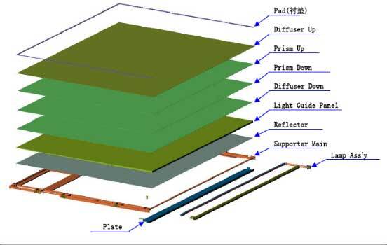
2. The structure and working principle of TFT-LCD Backlight
(1)Lamp
It is the source of visible light generated by receiving high voltage from an Inverter (reverse alternator), mainly using LED(light-emitting diode).
(2)Lamp housing
The light source reflected from the Lamp is incident on the light guide plate. Thin films with Ag and other materials attached to brass are used for reflection.
(3)Light guide panel
It is mainly made of propylene (PMMA) by Injection Molding or Casting method and has the function of guiding incident light source and uniformly distributing light source.
(4)Reflector
Polyether (PET) equipment mainly reduces the loss of light source incident on the light guide plate and has a reflection function.
(5)Diffuser Down (Diffusion Sheet)
It is mainly a spherical shape formed by propylene resin on polyether (PET) equipment, which uniformly diffuses the light source from the light guide plate and plays the role of collecting light at the same time.
(6)Bottom Prism
It mainly uses propylene resin to form a prism shape regularly and collect light on Polyether (PET) equipment. The brightness increase rate is 1.55 times that of the surface.
(7)Top Prism
It has the same function as Bottom Prism and increases the brightness by 1.33 times of Bottom Prism surface.
Prism collects light sources in X-axis and Y-axis directions in a cross-cross arrangement.
(8)Diffuser Up (Protective Film)
It has the same structure as the Diffuser Down, and its main purpose is to protect Prism, which is also called protective film. The light source of the Top Prism concentrated light is lost to some extent because of using the transmittance of the Diffuser, but it can reduce the bad characteristics of the Prism.
2. The manufacturing process of TFT-LCD
1. Manufacturing process of thin film transistor (TFT)
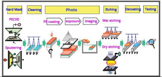
There are 6 processes of TFT manufacturing: Hard Mask, Cleaning, Photo, Etching, Decoating, and Testing. As shown in the figure.
(1) Hard Mark process
The hard mark process refers to the process of forming a film on Glass by using Gate electrodes, Data (Source/Drain) electrodes, pixel electrodes, insulating films, protective films, and semiconductor films through physical or chemical methods.
The Gate electrodes, Data (Source/Drain) electrodes, and Pixel electrodes are metal materials (aluminum, chromium, ITO, molybdenum), and the Target material is attached to Glass in the Plasma (ion region) between Target (mainly metal) and Glass by Sputtering physical method. Plasma (ion region) is formed by ionization by applying high voltage to inactive Gas implanted between two electrodes. Ionized inactive Gas is impacted on the Target, and then the detached Target material transfers to Glass to form the mask.
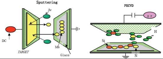
The insulating film, protective film, and semiconductor film are formed on Glass by the chemical PECVD (Plasma Enhanced Chemical Vapor Deposition) process. It is Plasma generated by injecting Gas between two electrodes and applying a high-frequency power supply.
(2) Cleaning process
The cleaning process refers to removing the pollution and Particle of Glass or membrane surface in the initial input or process in advance to avoid a bad process. It is helpful to ensure adhesion between films. The main units are the UV cleaning unit, Brush cleaning unit, Mega Sonic unit, and CJ (Cavitation Jet) unit.
(3)Photo process
The photo process refers to the operation in which the Mask formed on the film passes through light, the shape of which moves from Mask to Photoresist (PR), including the processes of PR Coating, exposure, and imaging.

(4) Etching process
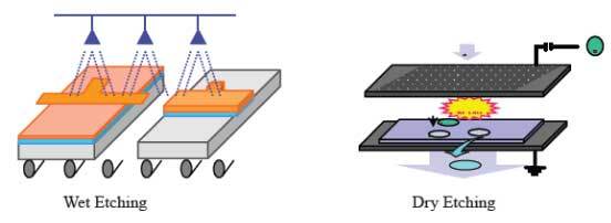
The etching process refers to the process of selectively removing the film with Photoresist (PR) by physical and chemical methods. There are two etching methods as follows: 1. Wet Etching is a method of etching metal substances (aluminum, chromium, ITO, molybdenum) by chemical solution; 2. Dry Etching uses Gas Plasma to etch SiNx and a-Si.
(5) Decoating process
The decoating process is a process of removing the Photoresist (PR) left to form a Pattern after the etching process.
The necessary condition of the decoating process is that PR is completely removed, the lower film should be intact, and the surface state for the next process should be maintained uniformly.
(6) Testing process
The testing process refers to the investigation/evaluation process, in which the quality of semi-finished products and products is evaluated.
2. Liquid crystal Box/Cell-making process
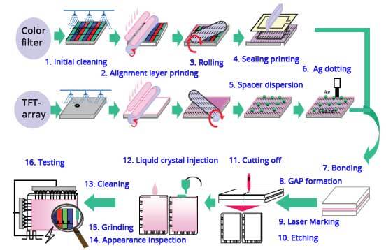
For the assembly process of the TFT-LCD panel (screen), firstly, the cleaned color film substrate and TFT array substrate are coated with alignment film coating solution and are oriented by friction. Then the array substrate of the TFT is coated with sealing glue, and spacers with a size of 5-10 μ m are scattered on the array substrate as supporting points. Afterward, the array substrate and the color film substrate are assembled and sealed with sealing glue to form an empty box (Cell).
Subsequently, the liquid crystal is injected into the cell in two ways. One way is to cut and split the empty cell substrate, take the required size of the final display product, inject the liquid crystal material after it has been evacuated and seal it after inspection. Another method is to inject liquid crystal first, then cut the piece and seal it again. The two methods’ production times are different, influencing the total pass rate and causing different production capacities.
3. Process flow of module
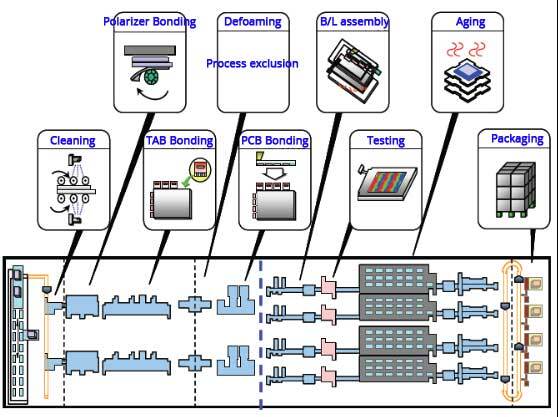
Finally, the panel of TFT-LCD is assembled with Drive IC and printed circuit board, and the liquid crystal module (LCM) is completed by installing a backlight and fixing the frame. The process includes polarizing plate bonding, TAB bonding, PCB bonding, B/L assembly, aging test, and packaging, as shown in Figure. In addition, each LCM should be inspected before and after aging.
(1) Polarizer bonding
It is mainly divided into two major processes: cleaning and bonding of polarizers.
Cleaning includes knife washing, brushing, rinsing, and drying: Knife washing is to remove glass debris with a rotating blade; Brushing is to remove dust and fingerprints with a brush; Rinsing is to remove residual impurities with pure water; Drying is to remove fine water vapor with high and low-temperature hot air.
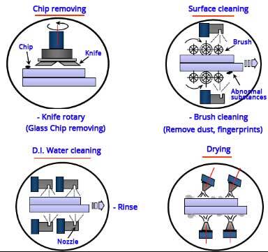
Polarizer bonding means that the upper and lower polarizers are respectively attached to the upper and lower panels by using the source on the Panel and the polarizer.

(2) TAB bonding
TAB bonding means using ACF (Anisotropic Conductive Film) to connect TAB (Tape Automated Bonding) with the Panel. The process includes ACF attachment, TAB positioning, and pressing: ACF attachment refers to attaching ACF to the Panel; TAB positioning is to pre-press TAB on the Panel by using the positioning source on the Panel; Pressing means the TAB is completely pressed on the Panel under high temperature and high pressure and make the ACF at the connecting part conducive.
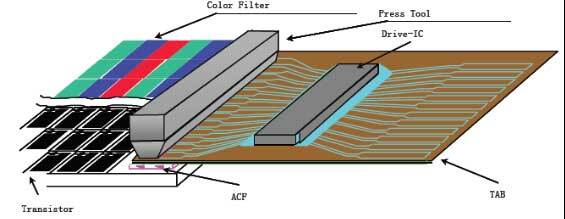
(3) PCB bonding
Like TAB bonding, PCB bonding is also connected by ACF. The ACF used is different due to different materials, and the engineering conditions are also different. The processes are divided into resin screen coating, ACF bonding, and PCB formal pressing. Resin screen coating is to prevent moisture and other abnormal materials from entering the Panel; ACF bonding is to attach ACF to the PCB panel; PCB formal pressing is to press PCB and TAB under high temperature and high pressure and make the ACF at the connecting part conductive.
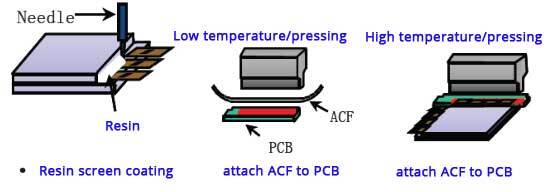
(4) B/L assembly
B/L assembly is a process of connecting the Case Top, Panel connecting TAB and PCB, Back Light, and Support Main by hand.
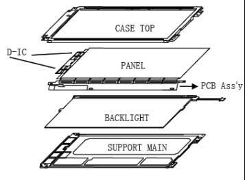
(5) Aging test
The aging test is to put the assembled liquid crystal module in an aging room at 50 ℃ to test the connection status of the module, and the aging time is different according to customer requirements.
(6) Packaging
The qualified LCD module is packaged and delivered by hand.
3. The characteristic indicator of TFT-LCD
1. Response time
Response time is an important indicator to measure the quality of TFT-LCD, which refers to the response speed of TFT-LCD to input signals, that is, the response time of liquid crystal from dark to bright or from bright to dark. Generally speaking, it is divided into two parts: Tr (Rise Time) and Tf (Fall Time), and the response time is the sum of the two. The smaller the response time, the better. If it exceeds 40 milliseconds, the moving image will be hysteresis. At present, the standard response time of TFT-LCD is about 25 milliseconds, but a few models can reach 16 milliseconds. With 16ms ultra-fast response time, it can display more than 60 frames per second. It means it can completely solve the problems of ghost images and trailing smears existing in traditional LCD screens when playing games or watching DVDs.
2. Contrast
Contrast refers to the brightness ratio between the bright area and the dark area of the display screen under the specified lighting conditions and observation conditions. Contrast is a parameter that directly reflects whether the TFT-LCD can present rich color levels. The higher the contrast, the better the layering of the restored picture. Presently, the nominal contrast of TFT-LCD is 250: 1 to 500: 1, and high-end products have a contrast of above 1000: 1. What should be explained here is that contrast must be matched with brightness to produce the best display effect. A high contrast ratio of 400: 1 or 500: 1 will make the display more colorful and softer, and the display effect of playing games or watching movies can be comparable to a CRT display.
3. Brightness
The brightness of LCD screen is generally higher than that of traditional CRT display screen, and the brightness of TFT-LCD is generally in cd/m2 (lumens/square meter). The higher the brightness, the stronger the anti-interference ability of the display screen to the surrounding environment, and the brighter the display effect. This parameter should be at least 200cd/m2, preferably above 1000cd/m2 for industrial applications. The higher the brightness of the traditional CRT display screen, the greater its radiation. The luminance of TFT-LCD is obtained by the illumination of the LED (light-emitting diode) backlight, so there is no negative impact on the human body.
4. Dead pixel
The most common dead pixels on the screen are white spots or black spots. The whole screen can be adjusted to a white screen to identify black spots, leaving the black spots nowhere to hide; White spots are just the opposite. The white spots will be discovered if the screen is adjusted to black. Usually, the display screen with no more than three dead pixels is qualified to leave the factory. The display screen with less than three dead pixels is a class-A screen; the display screen with more than three dead pixels but less than 10 is a class-B screen; the display screen with heavy spots and lines is a class-C screen.
5. Visual angle
TFT-LCD is a backlight display device, and the light emitted by the backlight behind the LCD module inevitably leads to the only best viewing angle-facing up. When you look at TFT-LCD from other angles, color distortion will happen because the backlight can penetrate the next pixels and enter the human eye. The undistorted range is the visual angle of the LCD screen. The viewing angle of TFT-LCD is also divided into horizontal viewing angle and vertical viewing angle, and the horizontal viewing angle is generally larger than the vertical viewing angle. At present, as long as the horizontal viewing angle reaches 120 degrees and the vertical viewing angle reaches 140 degrees, the screen can meet the demands of most users. The latest TFT-LCD panel is produced with wide viewing angle technology, which can reach 140 degrees from top to bottom and 150 degrees from left to right, thus reducing the inconvenience caused by the small viewing angle. Of course, this performance can’t be compared with a CRT display with a viewing angle close to 180 degrees, but it is more than enough for most applications.
6. Pixel spacing
The pixel spacing of TFT-LCD refers to the interval between each pixel of the LCD screen. Currently, the standard pixel spacing of mainstream (16:9) 23.6-inch TFT-LCD products is generally 0.276 mm, and the corresponding resolution is 1920 × 1080.
7. Bandwidth
The bandwidth of TFT-LCD is also an indicator to measure the LCD screen. Generally, the bandwidth of TFT-LCD is 80MHz. The large-screen TFT-LCD has the advantages of liquid crystal display and large-screen display, which makes the large-screen LCD products represented by 23.6-inch TFT-LCD favored by consumers. In addition, its visible area is larger than that of 24-inch color TV. Moreover, it has the advantage of no radiation, which can make users watch it at close range.
8. Thickness
Since the panel thickness of TFT-LCD is the same, the main factors influencing the thickness of TFT-LCD will be the circuit control panel’s technology, the plastic shell’s design, and the compression of internal space. Of course, with the integration of a few cutting-edge liquid crystal technologies, the latest ultra-thin liquid crystal panels, thinner high-brightness LED technology, coupled with more integrated control IC design and more optimized heat dissipation treatment, the overall size of the product can be significantly reduced.
4. Research progress and application of TFT-LCD
1. Current technical level of TFT-LCD:
(1) Both horizontal and vertical viewing angles can reach more than 170 degrees;
(2) The display brightness reaches more than 1000 nits, and the contrast ratio is more than 1000: 1;
(3) The life span exceeds 50,000 hours;
(4) Field sequence full color (FSFC) technology has been applied to industrial production;
(5) Large-screen TFT-LCTV has begun to enter large-scale industrial production. The image quality of TFT-LCTV has reached or even exceeded CRT. For example, the resolution of the 86-inch TFT LCTV is 1920 × 1200, and its horizontal and vertical viewing angles are 170 degrees; The 100-inch TFT LC TV has been successfully developed and commercialized.
(6) Large-area low-temperature polysilicon TFT-LCD has been successfully developed and put into industrial production, and amorphous silicon TFT self-scanning LCD has been commercialized;
(7) Reflective TFT-LCD color display is beginning to be commercialized. For example, a 5.8-inch reflective display with a resolution of 400 × 234 and a picture ratio of 16: 9 has a reflectivity of 30%, a response speed of 30ms, and a power consumption of 0.15 watts.
(8) The production line of 86 inches (about 1922 * 1093mm) substrate large screen has been successfully developed, and the production line of a larger substrate large screen is under construction.
(9) TFT-LCD with plastic substrate began to be commercialized. There are five kinds of plastic substrate products in Japan.
(10) Backlight and inverter. Although reflective LCD is being actively developed, transmissive TFT-LCD with backlight will still be the mainstream product for a long time. The backlight is an essential accessory. Germany has developed a flat fluorescent lamp backlight for liquid crystal modules, with a brightness of 5000-7000cd/m2 and a life of 100,000 hours. Some new self-heating backlights can normally work in the range of-40 ℃ to 85 ℃. OEL backlight and high brightness LED backlight have been successfully developed and started to be used in TFT-LCD, Linfinity. Microelectronics invented a long-life inverter with cold cathode backlight, the modulation range of the light source of which reaches 500: 1.
2. Application of TFT-LCD
TFT-LCD is mainly used in computers, video terminals, communication, instrumentation, and other industries. The main application fields are laptops, desktop computer monitors, workstations, industrial monitors, global positioning systems (GPS), personal data processing, game consoles, portable VCDs, DVDs, and other portable devices.

